
I am Endong Dai, a Master’s student in Electrical and Computer Engineering (Hardware Track) at Duke University. I focus on Digital IC RTL design, VLSI Layout Design and PCB development, with experience in Verilog, C/C++, Altium Designer, and Virtuoso . Strong foundation in power electronics and embedded system, backed by research in AI chip design and floating-point ALU implementation. Passionate about creating efficient, high-performance hardware architectures bridging digital logic and system integration. You can find more information through my CV.
Interested in:
- ASIC/FPGA RTL Design
- VLSI Layout
- PCB
🎓 Education
Duke University — Durham, NC, USA
M.S. Electrical and Computer Engineering (Hardware Track) — GPA: 3.8/4.0
Aug 2025 – May 2027 (expected)
Research: Duke Center for Computational Evolutionary Intelligence (Duke CEI), Advisor: Prof. Yiran Chen
University of Nottingham (China + UK 2+2 Program)
B.Eng. Electrical and Electronic Engineering — First Class Honours, GPA: 3.8/4.0
Sep 2021 – Jul 2025
Awards
- Dean’s Scholarship
📄 Publications
- C. Zhou, …, E. Dai (4th author), …, “NPU accelerator for image generation,” IEEE International Solid-State Circuits Conference (ISSCC), 2027. Accepted.
- V. Wang, C. Zhou, E. Dai, H. Li, and Y. Chen, “BinSel: Sort-free top-k selection for sparse vision attention from rotated 1-bit keys,” IEEE International Symposium on Circuits and Systems (ISCAS), 2027. Under review.
- Y. Zhong, C. Zhou, Z. Xu, E. Dai, et al., “Training-free spatially selective acceleration for coarse-to-fine 3D generation,” International Conference on Learning Representations (ICLR), 2027. Under review (double-blind).
👨🏫 Teaching
Teaching Assistant — Duke University
Department of Electrical & Computer Engineering
Summer – Fall 2026
- Led an RTL Design Workshop (Summer 2026), guiding students through Verilog modeling and simulation.
- Course TA for ECE 550 — Fundamentals of Computer Systems and Engineering (Fall 2026): held office hours, graded assignments, and mentored students on RTL design and verification.
🔧 Hardware Skills
IC & FPGA Design
- Verilog / SystemVerilog (RTL Design & Verification)
- FPGA Prototyping & Bring-Up (Xilinx ZCU102)
- Vivado, Quartus Prime, Synopsys VCS, Cadence Xcelium
- Cadence Virtuoso (Digital & Analog/Mixed-Signal IC Layout)
Verification
- UVM
- AMBA AXI / AXI-Stream
PCB & Simulation
- Altium Designer & KiCad PCB Design
- LTspice
- PLECS
- MATLAB / Simulink (control-loop design & modeling)
- Soldering
Programming & Embedded
- C / C++
- Assembly (PIC16, MIPS)
- STM32 (STM32CubeIDE)
- Eclipse (Xilinx Vitis)
- Arduino
- Raspberry Pi
- ROS
Tools & Platforms
- Claude Code
- Linux (Ubuntu)
- Git
💻 Selected Projects
LLM Accelerator – Matrix Multiplication Unit (MMU)
Duke University - Duke Center of Computational Evolutionary Intelligence (CEI)
Jan 2026 – Jun 2026 · TSMC 16 nm, 2 mm × 2 mm die (not yet taped out)
Architected the Matrix Multiplication Unit (MMU), the central GEMM/GEMV engine of an LLM accelerator. The key idea is to use K-means codebook (vector) quantization to recast the memory-bound decode GEMV into a dense GEMM, achieving up to a 10× decode speedup while keeping a single shared PE array for both prefill and decode.
Core Idea — Codebook Quantization (GEMV → GEMM)
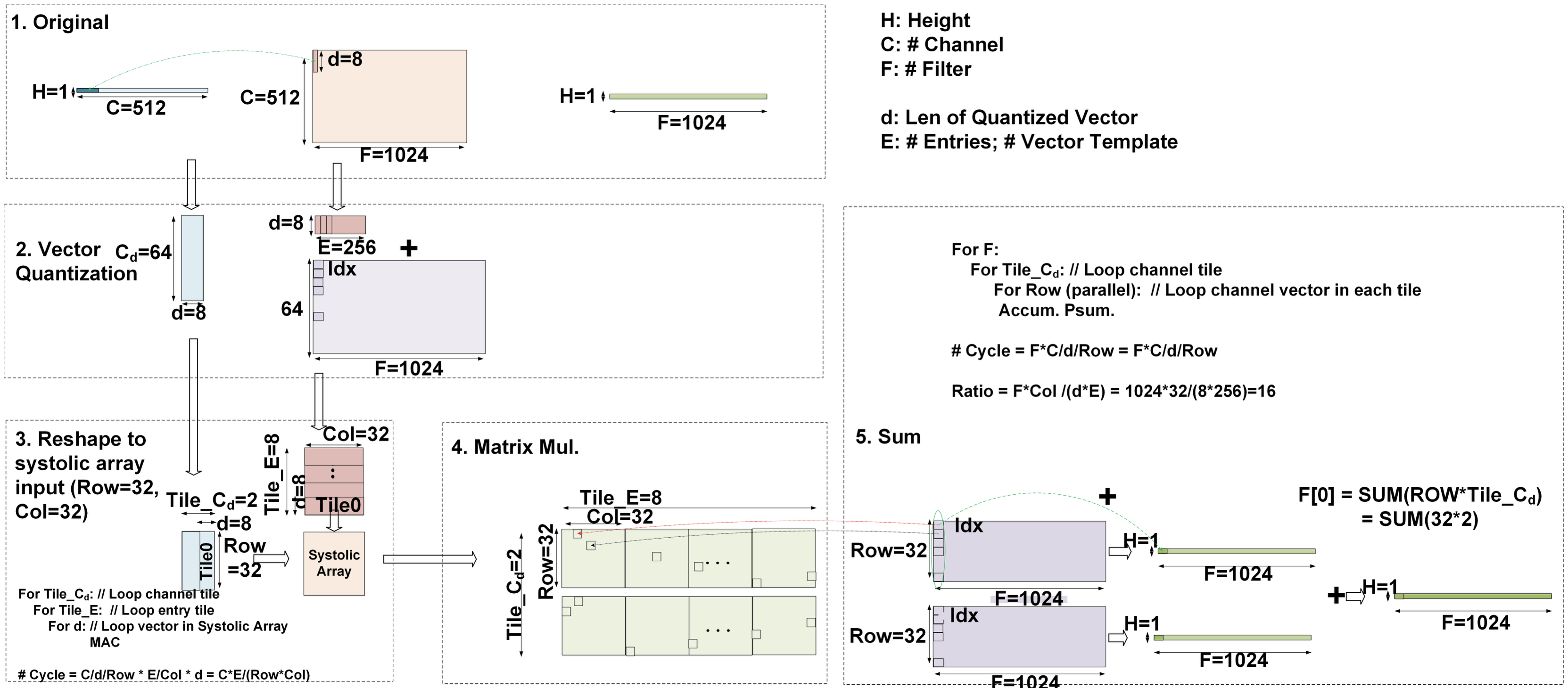
- Original GEMV is memory-bound: every decode step streams the full weight matrix (e.g.
C=512,F=1024) from memory, so bandwidth — not compute — limits throughput. - Vector quantization: weight vectors are clustered with K-means into a small codebook (
d=8length vectors,E=256entries). Each weight is replaced by an index (Idx) into the codebook, drastically shrinking the weight footprint. - Reshape to systolic input: indexed weights are tiled into the systolic array layout (
Row=32,Tile_C=32), turning sparse/irregular lookups into a regular dense tile stream. - Matrix multiply + accumulate: the codebook entries are matrix-multiplied once and reused across rows, so the heavy compute happens on the small codebook instead of the full weight matrix.
- Result: the effective work drops to
Ratio = F×Col + d×E = 1024×32 + 8×256 ≈ 16×fewer operations, delivering the ~10× end-to-end decode speedup.
Hardware Architecture & Dataflow
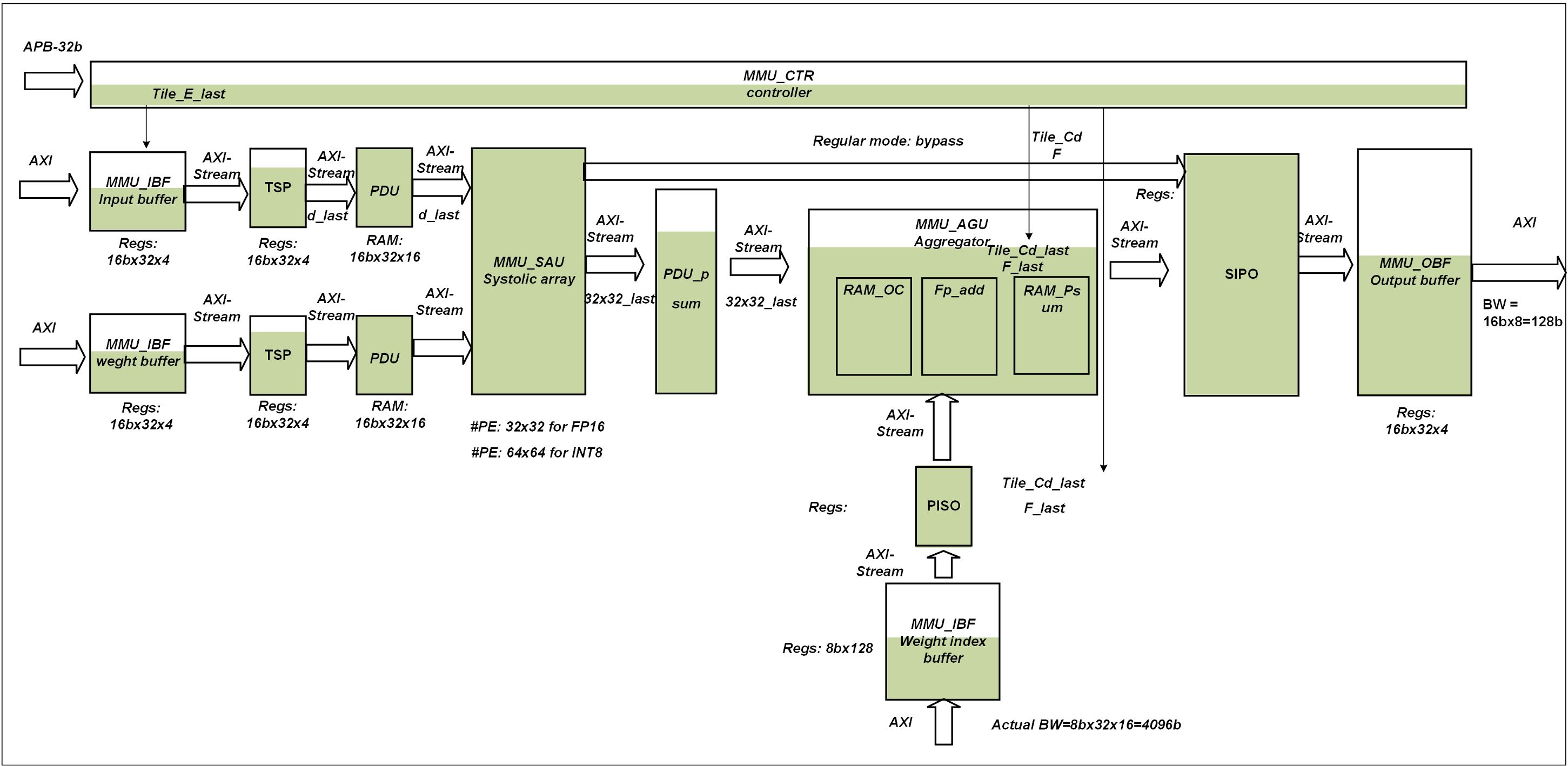
- Dual-mode datapath on a shared PE array, sequenced by the
MMU_CTRcontroller:- Prefill (regular mode): full-precision GEMM — the quantization path is bypassed.
- Decode (quantized mode): codebook-indexed GEMV computed as dense GEMM for optimized throughput.
- Systolic PE array (
MMU_SAU): a shared 32×32 INT4 / 16×16 FP8 PE array, fed by an AXI-Stream ready/valid dataflow for back-pressure–safe streaming. - Front-end staging: dual
MMU_IBFinput/weight buffers →TSP(transpose/skew) →PDU(phase delay unit) align operands into the row-skewed format the systolic array expects. - Back-end aggregation (
MMU_AGU):RAM_OC,Fp_add, andRAM_Psumaccumulate partial sums (Psum), with SIPO/PISO converters bridging serial and parallel AXI-Stream widths. - Weight index path: a dedicated
MMU_IBFweight-index buffer (actualBW = 8b × 32 × 16 = 4096b) supplies codebook indices for the quantized decode mode. - Performance & power: 1.024 TOPS (INT4) / 0.256 TOPS (FP8) peak at 500 MHz with 512 KB on-chip SRAM; estimated SoC power 0.810 W (MMU 0.345 W).
- Verification: verified across GEMM and VQ-GEMV modes, INT4/FP8 precisions, ISA parameters, and tile boundaries (270 test cases); the MMU stays busy for ~99% of end-to-end prefill and decode execution time.
Diffusion Chip – FPGA Validation & Post-Silicon SoC Bring-Up
Duke University - Duke Center of Computational Evolutionary Intelligence (CEI)
Feb 2026 – Sep 2026 · Taped-out TSMC 16 nm chip (ISSCC 2027)
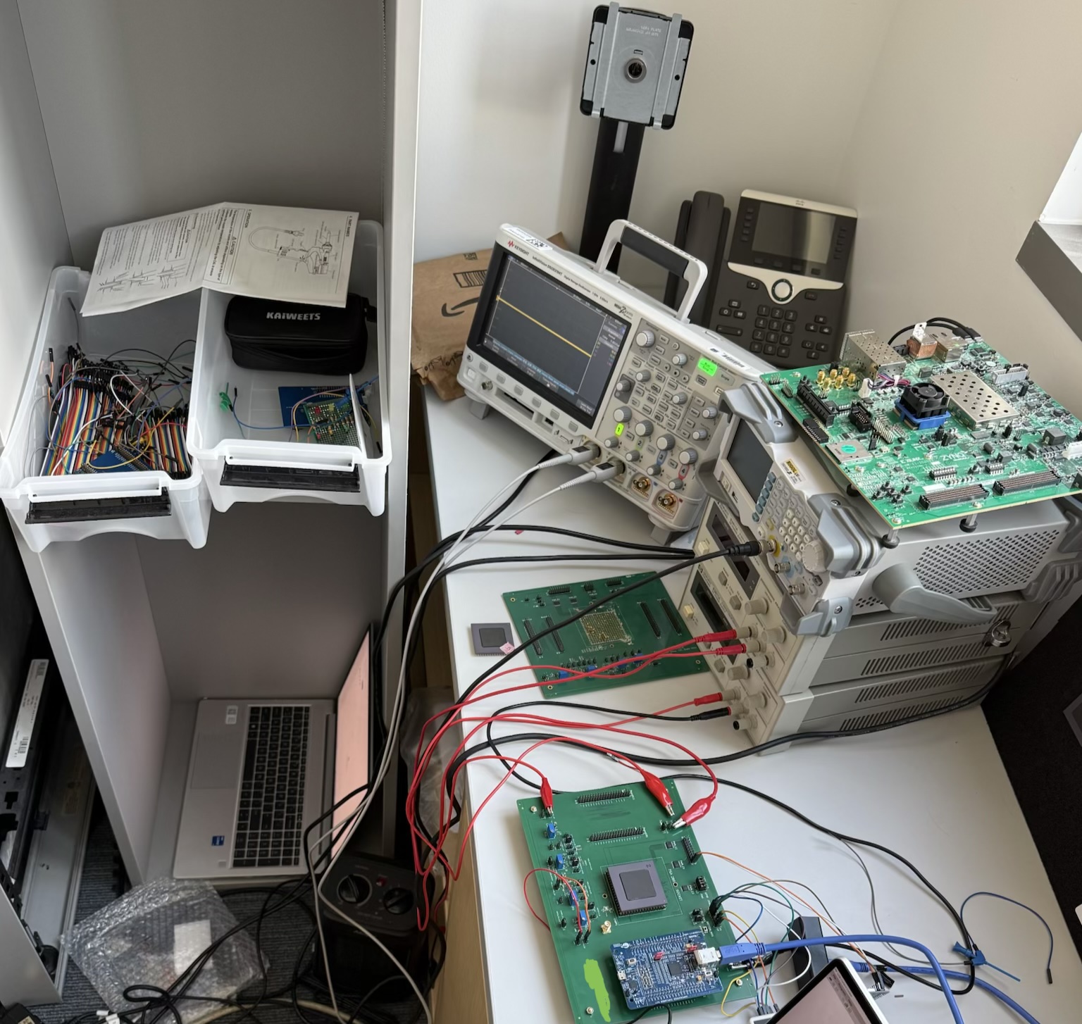
Drove backend productization and bring-up of the diffusion chip (TSMC 16 nm, CPGA-208): CPU/NPU, 1 MB GLB SRAM, GPIO, and dual 32-bit FX3 interfaces over a shared AXI fabric.
Bring-Up Test Bench
Model-to-Silicon Verification Flow
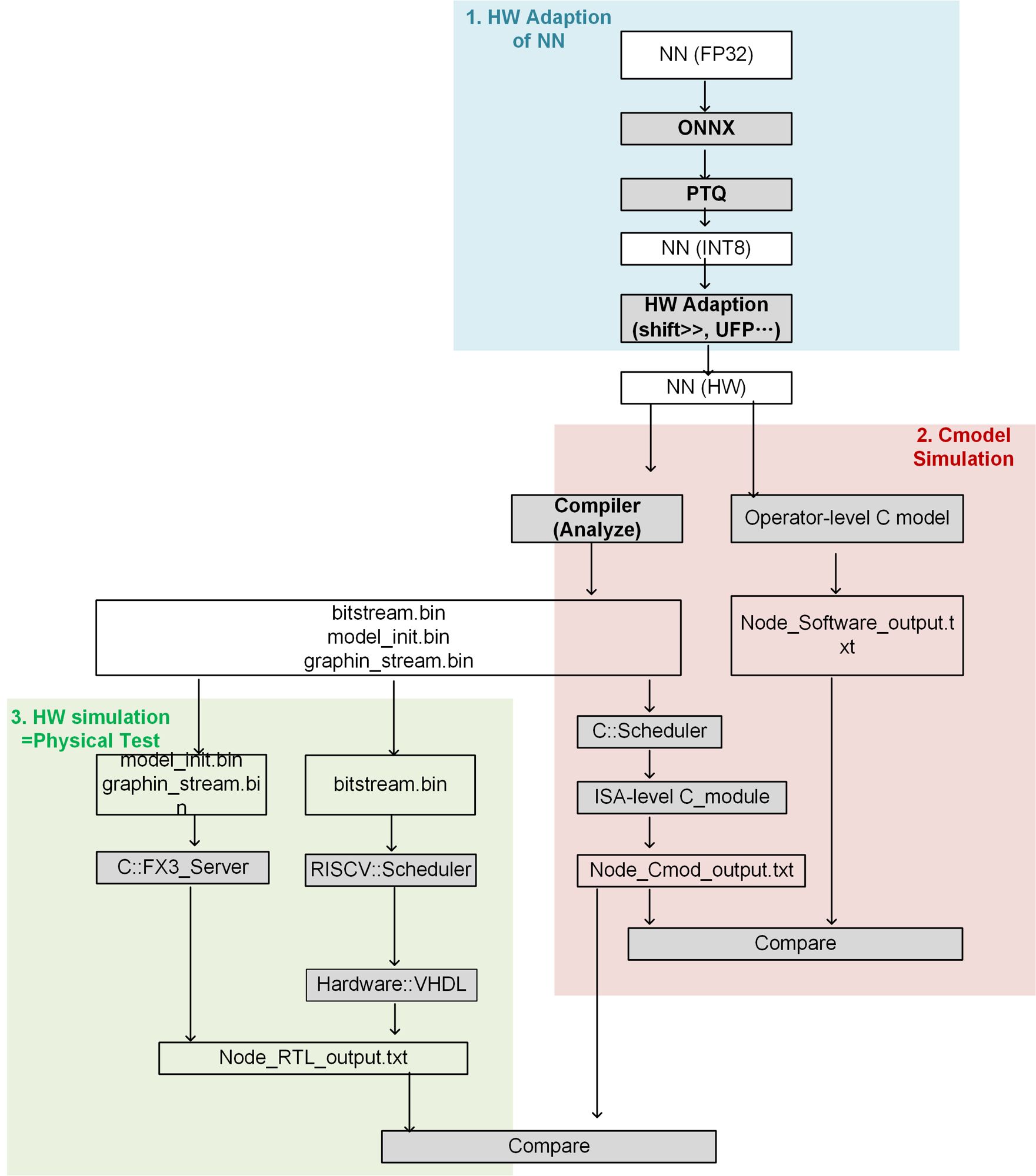
The diffusion NN is quantized (ONNX → PTQ → INT8) and hardware-adapted, then verified node-by-node across three paths — the operator-level C-model (software golden), the ISA-level C-model scheduler, and the hardware / physical run (FX3 server + RISC-V scheduler + RTL) — comparing every node tensor to localize any mismatch. This is the flow used to drive the full diffusion UNet — all 762 hardware-scheduled nodes — to bit-exact 0-mismatch on real silicon.
Key Contributions
- Deployed FPGA-based validation on AMD ZCU102 to verify PC-to-chip communication and control functionality through FX3, UART, JTAG, and GPIO interfaces during system bring-up.
- Performed post-silicon SoC validation on the taped-out chip, bringing up FX3 high-speed TX/RX links and running NPU and general-purpose operators on real silicon against software golden models.
- Brought up the full diffusion UNet on real silicon — all 762 hardware-scheduled nodes of an 839-node ONNX graph — reaching bit-exact 0-mismatch against the scheduler / C-model golden across 41K+ dumped node tensors.
- Root-caused and fixed 12 independent bring-up bugs across firmware operator scheduling, NPU hardware modes, and FX3 USB packet/ACK protocol, advancing the on-chip run from node n9 → full-model completion (n762).
Matrix Skew Unit for Systolic Dataflow (PDU) ▸ click to expand
Duke University - Duke Center of Computational Evolutionary Intelligence (CEI)
Sep 2025 – Jan 2026
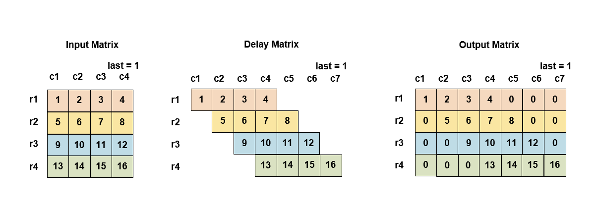
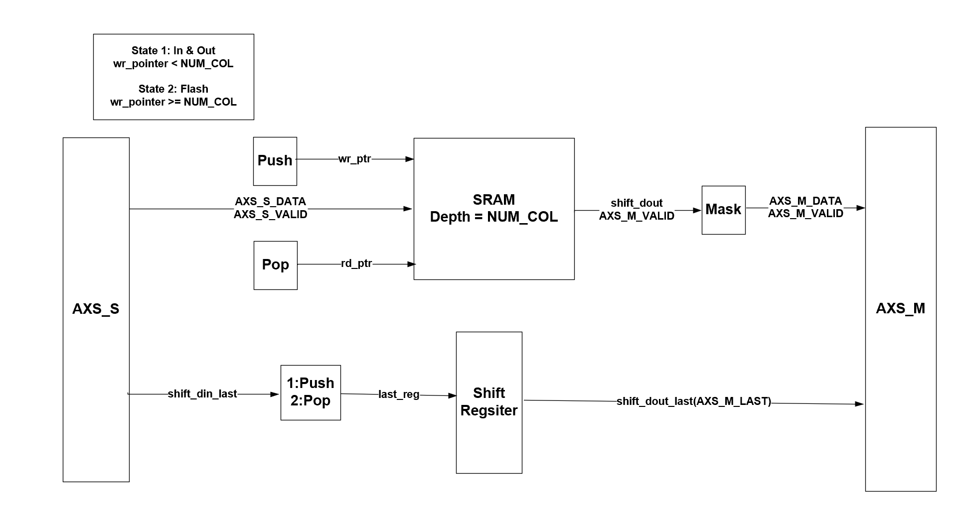
Designed a phase delay unit (PDU) for matrix data alignment, enabling row-wise skewed dataflow for systolic-style matrix computation.
PDU Dataflow
PDU Pipeline
Diffusion AI Chip – Gather/Scatter Unit (SGU) ▸ click to expand
Duke University - CEI
Sep 2025 – Jan 2026
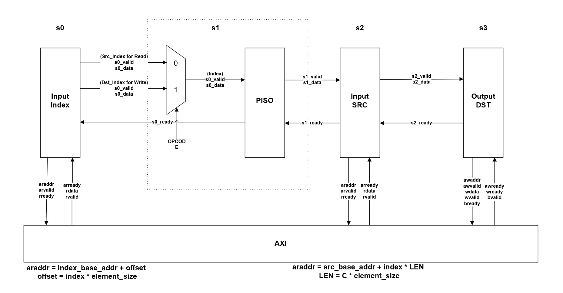
Designed a Gather/Scatter Unit for irregular memory access in diffusion AI accelerators with AXI interface.
Gather / Scatter Dataflow
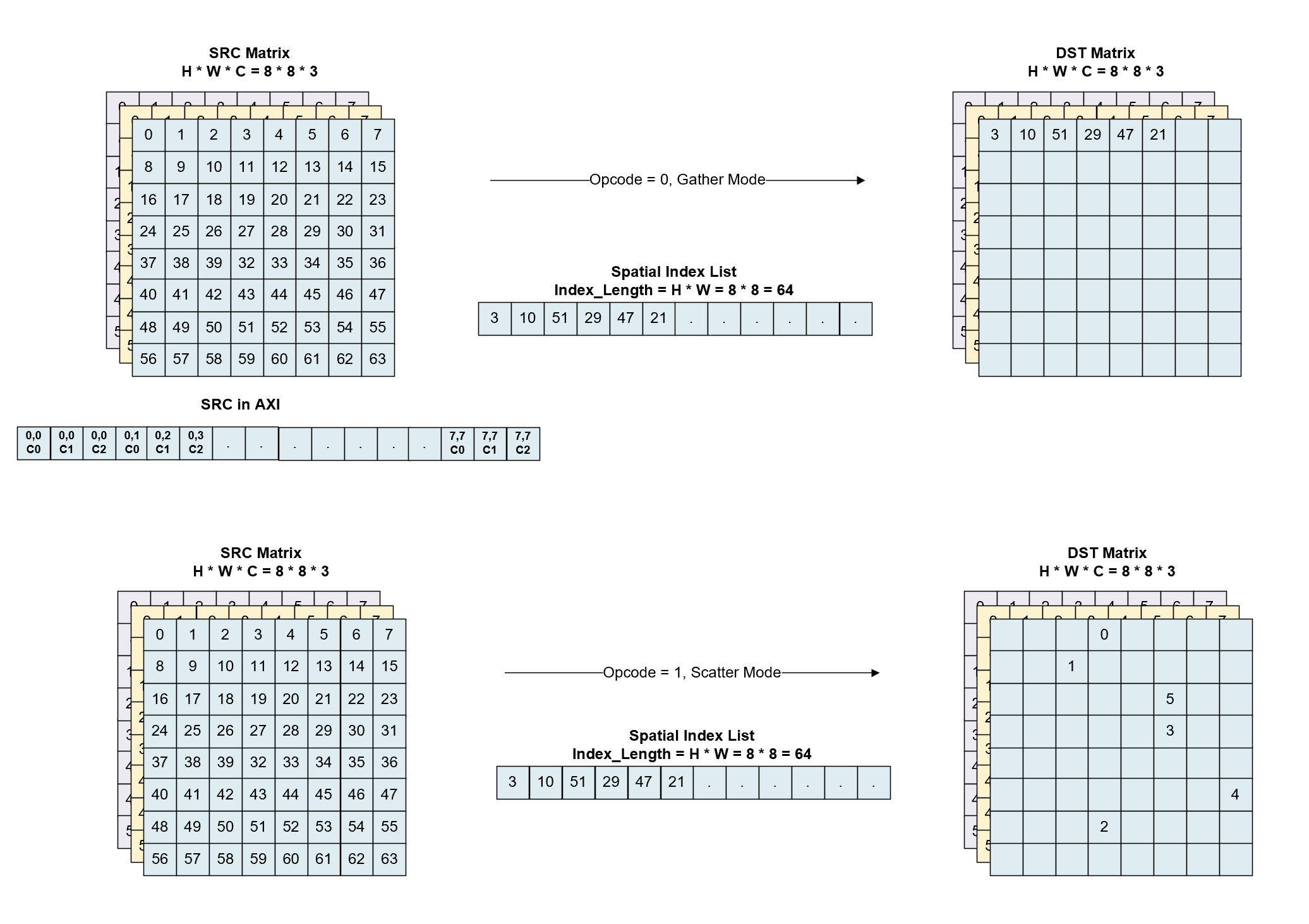
This diagram illustrates how the SGU performs gather and scatter operations using a spatial index list.
SGU Hardware Architecture (4-stage pipeline)
Diffusion AI Chip Tape-Out PCB (CPGA Socket Design)
Duke University - CEI
Mar 2026 – Present (v1 completed Apr 2026)
Designed a 6-layer PCB socket system for a 164-pin diffusion AI chip using a CPGA-208 package, enabling high-speed communication with dual USB FX3 boards and external debugging interfaces. Focused on signal integrity, delay budgeting, and power domain partitioning across chip-package-board co-design.
PCB Schematic & Layout
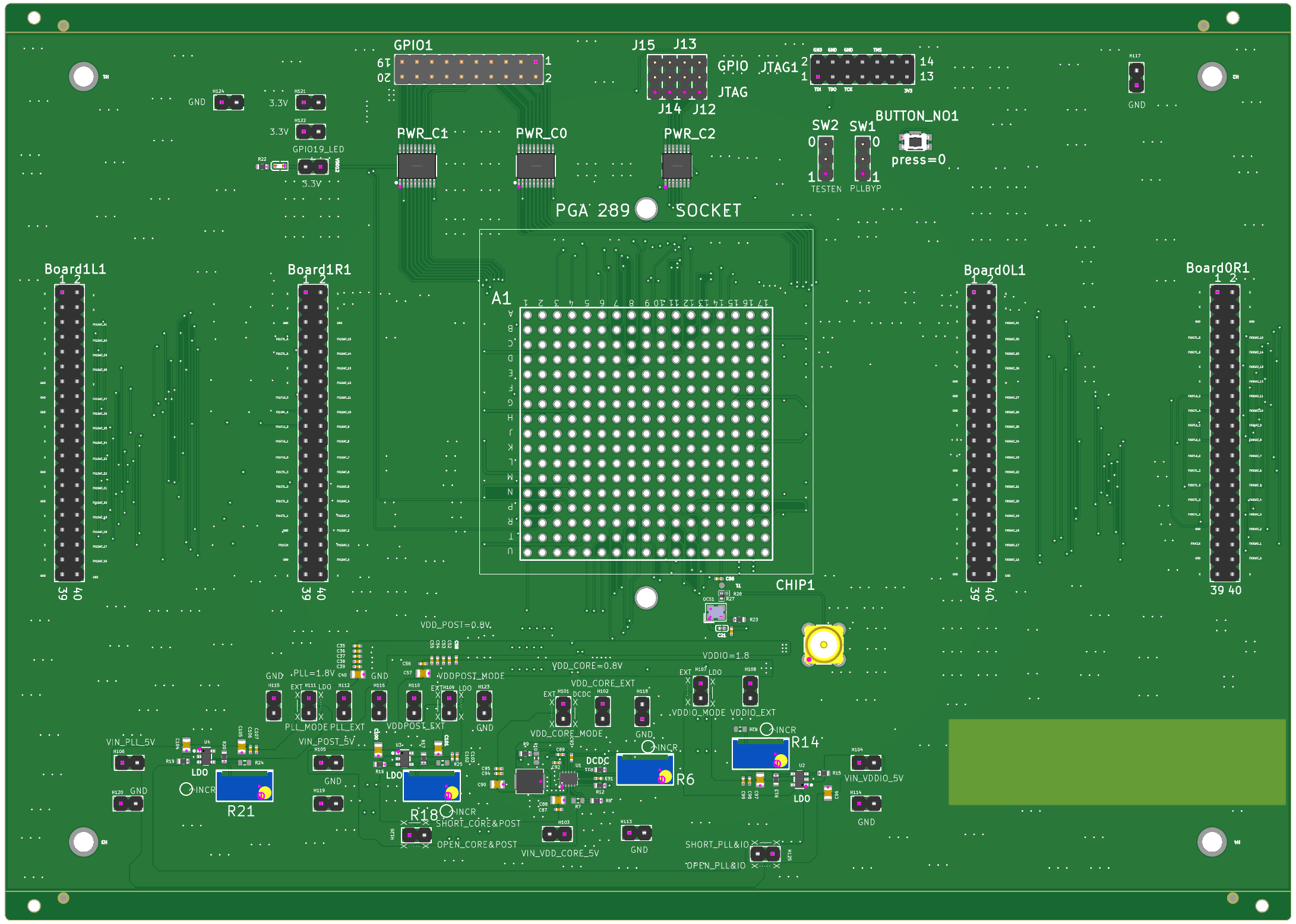
Key Contributions
- Designed CPGA-208 socket mapping and chip-to-board bonding interface for a 164-pin custom ASIC
- Implemented dual 32-bit high-speed interfaces (100 MHz) to USB FX3 boards with strict timing constraints
- Achieved length-matched routing (1800 mil ± 1 mil) to ensure signal skew minimization
- Performed end-to-end delay budgeting: PCB delay (0.3ns) + USB interface (0.7ns) + Chip Package delay = 2.5 ~ 3 ns system requirement
- Partitioned multiple power domains (VDDIO / VDD_core / VDDHV / VDDPOST) and designed stable power distribution network
- Completed full schematic + BOM (JLCPCB components) and 6-layer PCB layout in Altium Designer
IEEE-754 Half Precision Floating-Point ALU
Duke University
Sep 2025 – Dec 2025
Designed a 16-bit floating-point ALU supporting: ADD, SUB, MUL, DIV (Restoring Method)
Estimated performance (TSMC 65 nm):
- 16 MHz Maximum Frequency
- <18 mW Power Consumption
- 0.0083 mm² Divider Core Area
Divider Core Top-Level Schematic
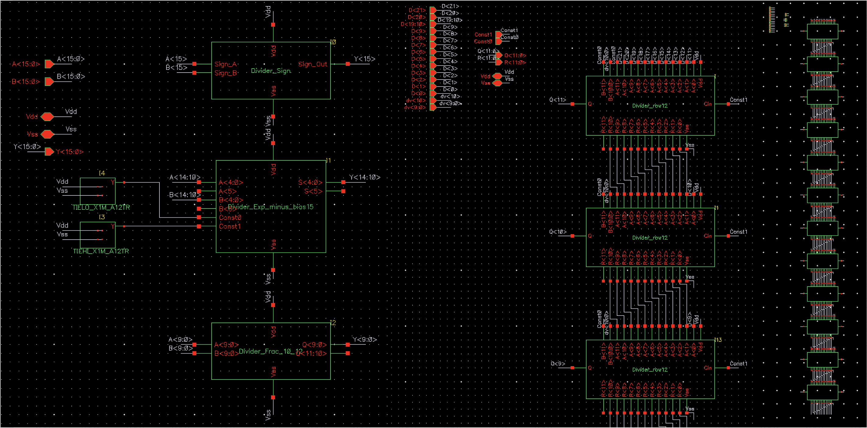
Top-level hierarchical schematic of the divider core showing sign processing, exponent logic, and fraction division datapath.
Divider Core Layout
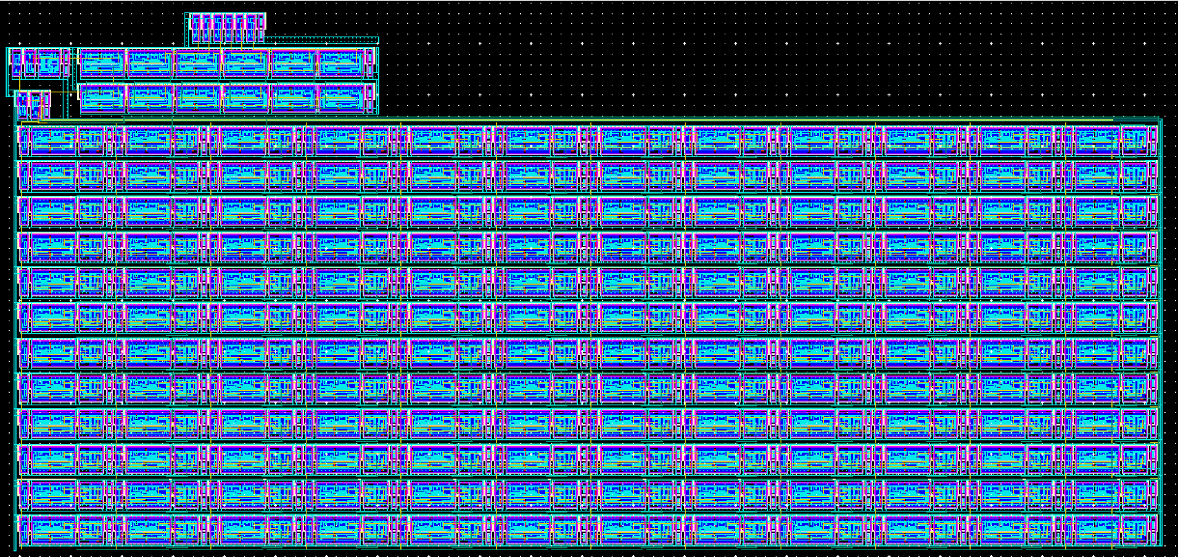
Standard-cell physical layout of the divider core implemented in a digital CMOS flow.
Multi-Channel FM Receiver with PLL-Based Tuning
Duke University
Jan 2026 – Apr 2026
Designed a multi-channel FM receiver in 65 nm CMOS using PLL-based frequency tuning for RF downconversion. The receiver supports FM-band input selection and generates corresponding LO frequencies for a fixed IF architecture.
Key features:
- RF input band: 88–108 MHz, with selected input channels at 88 / 96 / 102 / 108 MHz
- LO generation: 78 / 86 / 92 / 98 MHz for 10 MHz IF downconversion
- PLL reference clock: 2 MHz
- Supply voltage: 1.2 V
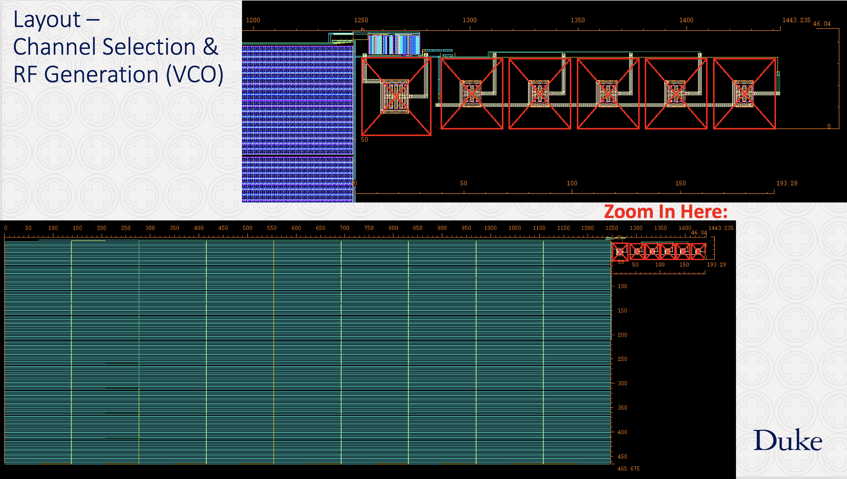
- Channel Selection & RF Generation (VCO) layout area: approximately 0.687 mm²
Key Contributions
- Designed and verified the multi-channel selection path, including resistor-tree voltage generation and 4-to-1 MUX channel selection.
- Implemented the OTA buffer, ring VCO, and PLL building blocks including phase detector and charge pump in Cadence Virtuoso.
Problem & Solution
One major layout challenge was the large area caused by the rppoly resistor-tree voltage divider, which significantly increased the top-level layout area. A possible improvement is to replace the large rppoly resistor network with more area-efficient resistor options, such as metal-to-metal resistor structures or alternative compact passive implementations, to reduce area while maintaining stable channel-selection voltages.
Receiver Architecture and Layout
Top-level schematic of the PLL-based multi-channel FM receiver, including channel selection, OTA buffer, VCO, phase detector, and charge pump blocks.
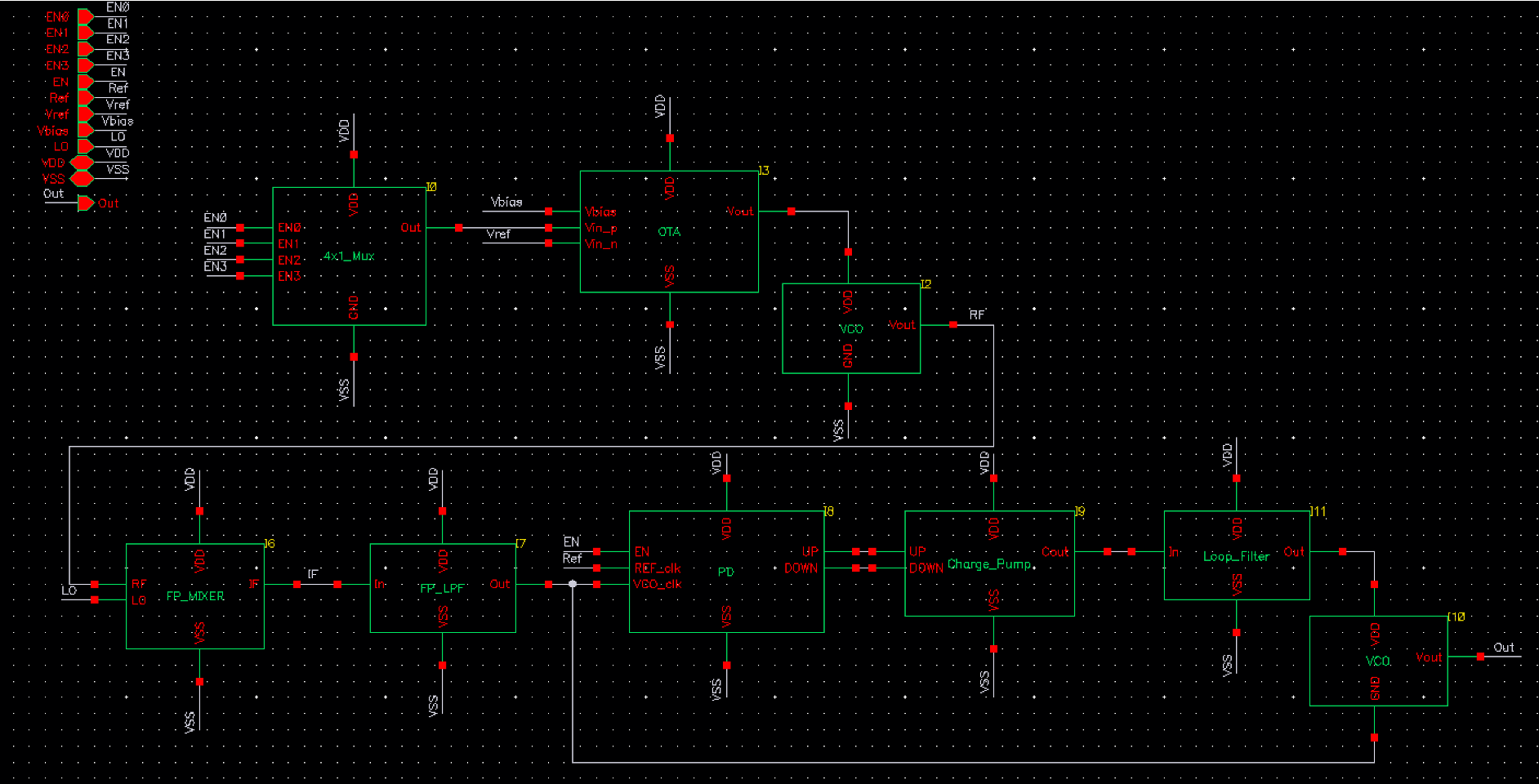
Layout of the channel selection and RF/LO generation section, including the resistor-tree voltage generation, 4-to-1 MUX, OTA buffer, and VCO tuning path.
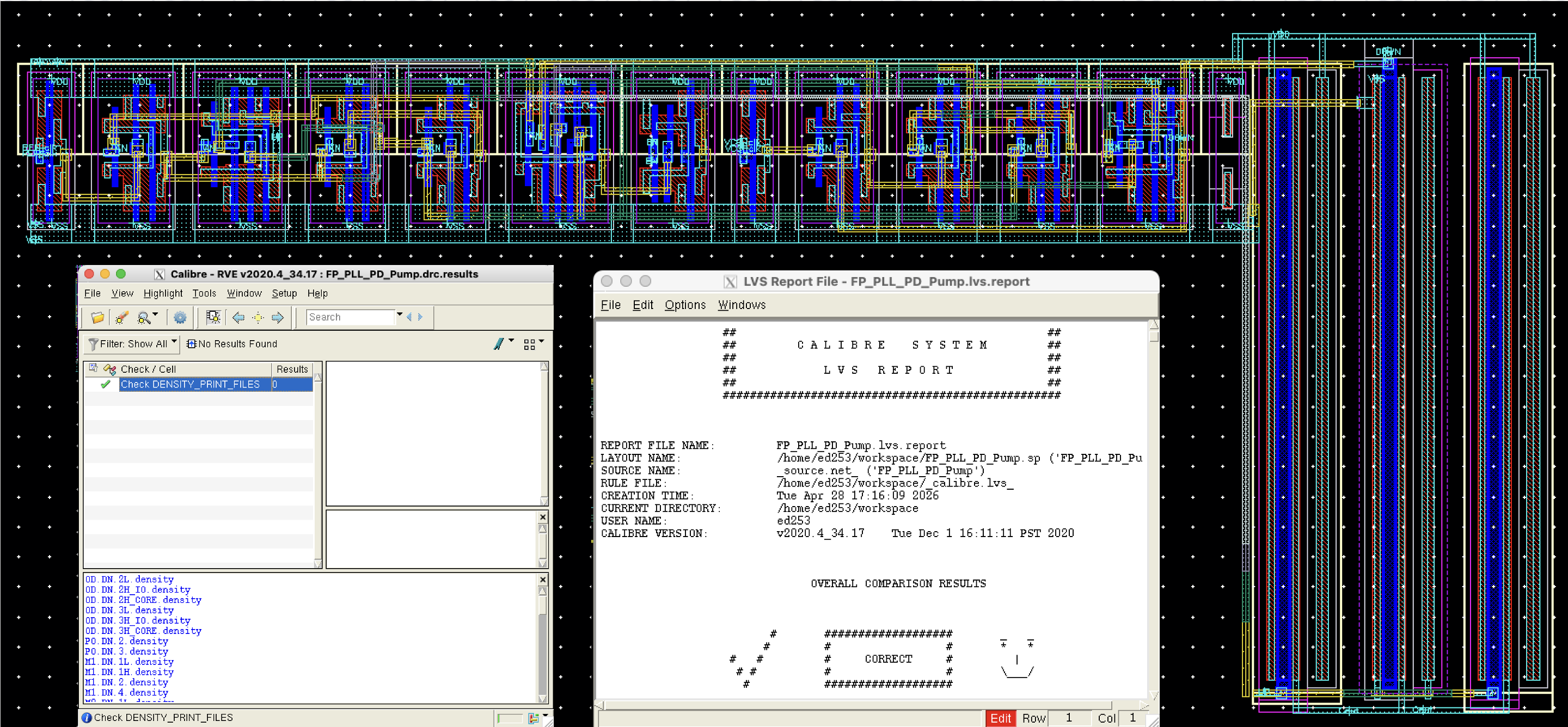
Layout of the PLL phase detector and charge pump blocks used for PLL-based frequency tuning.
High-Frequency Power Electronics Converter
University of Nottingham
Final Year Individual Project
Oct 2024 – May 2025
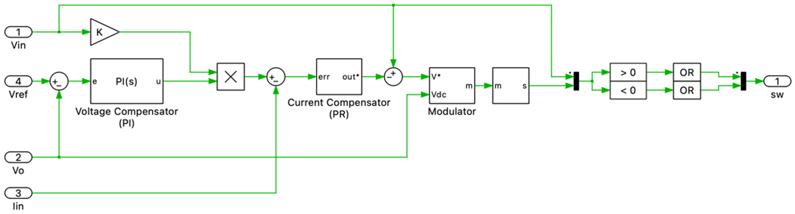
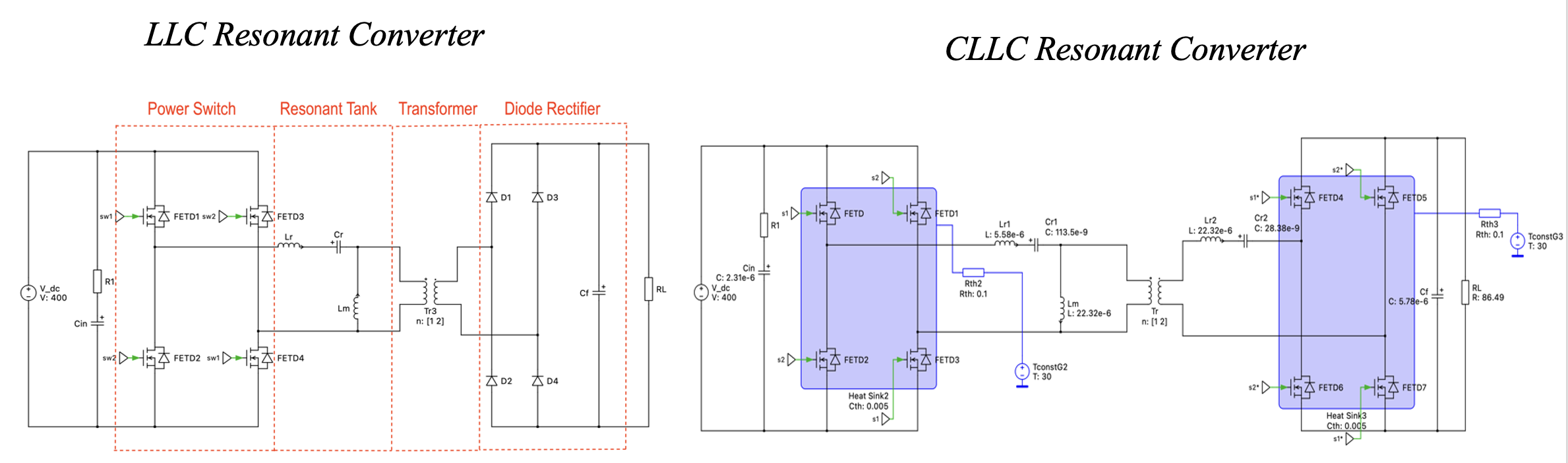
Designed and simulated a two-stage 7.4 kW / ~200 kHz on-board charger (OBC) for Electric Vehicles using SiC wide-bandgap devices, modelled in PLECS/MATLAB with per-device thermal models.
Key results:
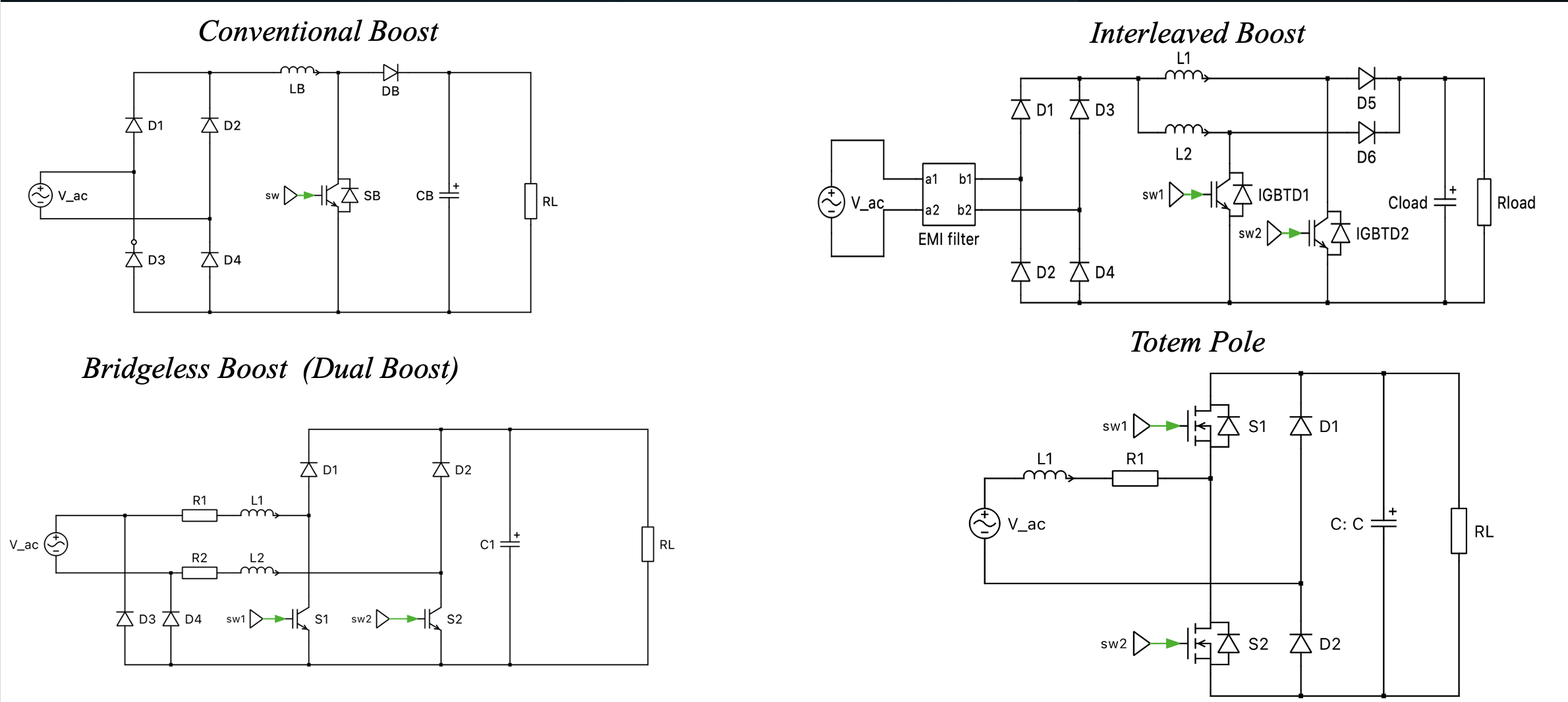
- Totem-Pole PFC front-end — power factor up to 0.98 (230 V) / 0.9951 (110 V), efficiency > 99% across load (peak 99.13%), current THD 0.21 (230 V) / 0.09 (110 V).
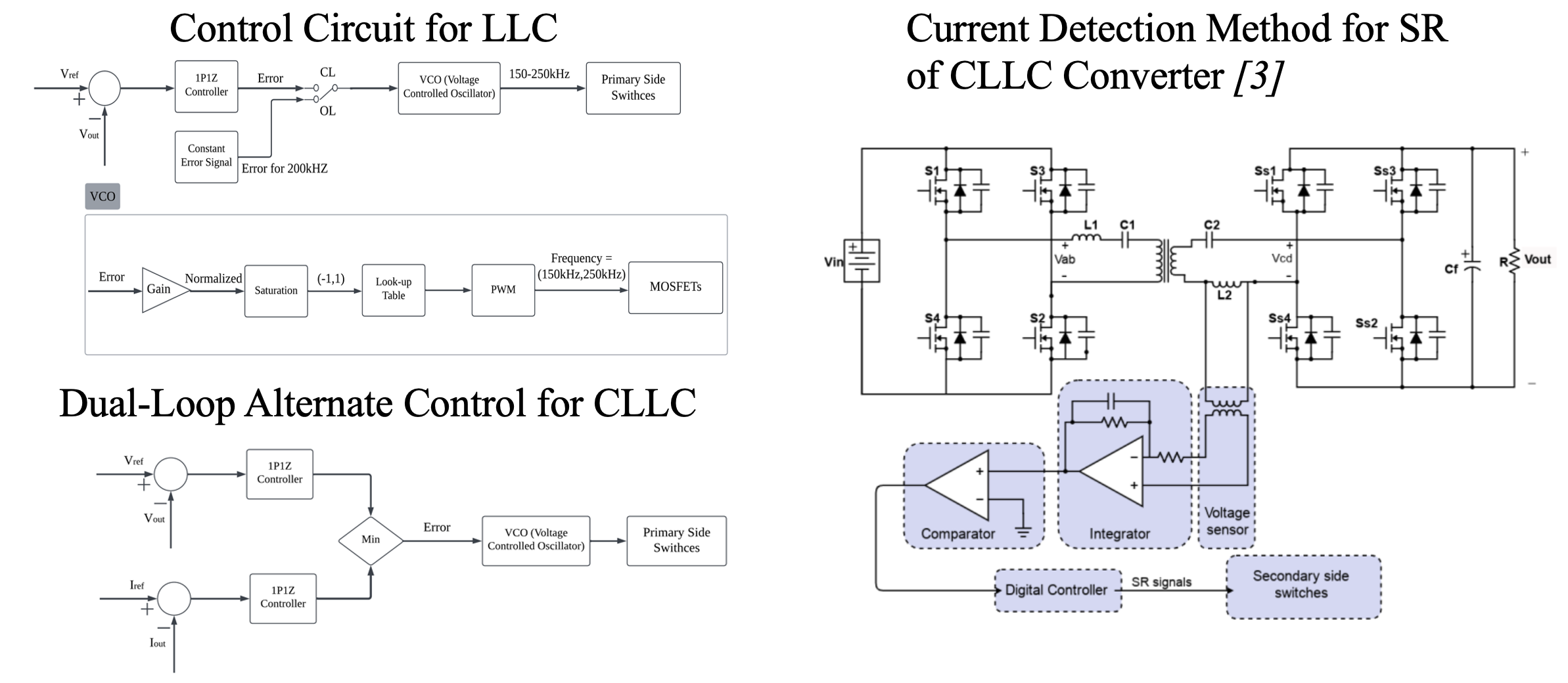
- CLLC resonant DC–DC stage — peak efficiency 99.9%, holding ≥ 99.75% even at 20% light load; closed-loop control cut total loss from 93.2 W → 26.6 W.
- Dual-loop PI + PR control — output-voltage regulation within ±5% (CLLC output within ±0.05%) across 20%–100% load and ±5% line variation.
- Evaluated efficiency, loss distribution, and thermal behaviour per SiC MOSFET/diode to confirm soft-switching and safe junction temperatures.
System Architecture
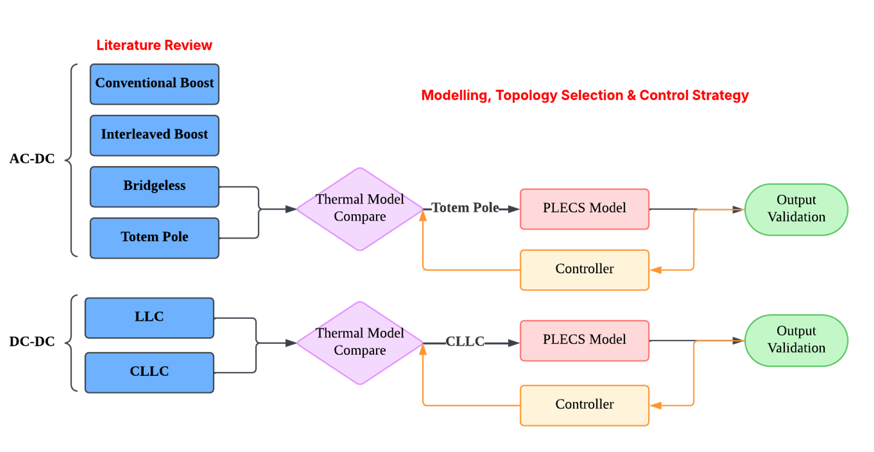
Two-stage architecture consisting of a Totem-Pole PFC front-end and a CLLC resonant DC–DC converter.
PFC Stage
DC-DC Converter Stage
Omni-Directional Robot Collision Awareness
University of Nottingham
Jun 2024 – Aug 2024
Implemented an autonomous robot navigation system using ROS and LiDAR-based SLAM.
Key work:
- Configured ROS Noetic + Gazebo + RViz simulation environment
- Deployed Cartographer SLAM for real-time LiDAR mapping
- Integrated RoboRTS navigation stack for autonomous navigation
- Implemented 2D mapping and navigation using LiDAR sensor data
LiDAR Mapping Result (IAMET Building)
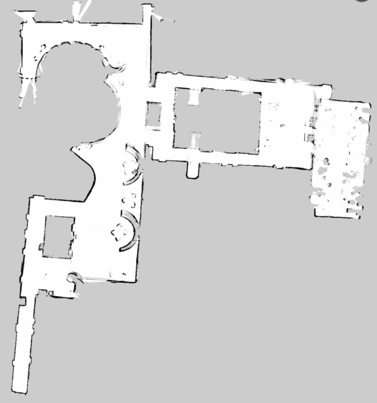
Final map generated by the Cartographer SLAM algorithm, reconstructing the layout of the second floor of the IAMET building using LiDAR data.
Heart Rate, Pulse Oximeter System
University of Nottingham
Oct 2023 – Dec 2023
Embedded biomedical device using STM32.
- Designed analog front-end circuits
- Implemented FFT-based heart rate detection
- Developed ADC firmware for signal processing
🎮 Have Fun(Game Demo)
Fire Emblem-Inspired SRPG Demo
Personal Project
Apr 2026 – Present
Developed a tactical role-playing game prototype in Python inspired by Fire Emblem-style grid combat. Implemented unit movement, attack range visualization, combat flow, terrain effects, chapter-based setup, and sprite-based rendering. Refactored the project for browser compatibility and deployed a playable web demo using pygbag and GitHub Pages.
Highlights
- Built a grid-based SRPG framework with chapter selection, unit actions, AI turns, and terrain effects
- Implemented movement/attack range overlays, inventory actions, combat preview, and faction-based rendering
- Restructured the Python project entry flow for both local execution and browser runtime compatibility
- Debugged web runtime startup issues and deployed a playable online demo
Demo: Play Project_Alpha
📬 Contact
Email
ed253@duke.edu
daiendong81@gmail.com
GitHub
https://github.com/endong-dai
LinkedIn
https://www.linkedin.com/in/endong-dai-607052385